
Voltage Topologies – Part 1 of 2
This article is divided into two parts. The first part covers the introduction of switching regulators and Non-isolated DC-DC converters like buck, boost, buck-boost (inverting), Cúk, and SEPIC converters.
Switching regulators revolutionized supply methods by drastically reducing power supply limitations and miniaturizing equipment. Control transistors operate in the linear active region in linear series and shunt regulators. The conduction of transistors is adjusted to obtain, maintain, and regulate the desired output voltage. The control transistor acts as a switch in a switching regulator, either in the saturation or cutoff. Regulation involves ON-time adjustment of the control transistor.
The control transistor’s power dissipation in this operational mode is lower than in linear types. Switching voltage regulators thus have superior efficiency and provide more significant load currents at low voltage than linear regulators.
Implementation of switching regulators needs different topologies such as flyback and forward. Factors like cost, performance, and application influence topology choice as most topologies are compatible with various applications.
Switching Converter Topologies
The switching topologies comprise two groups:
(i)Non-Isolated converters: Current can flow between input and output in this single circuit power converter. The lack of separation between input and output makes it cheaper.
(ii)Isolated converters: This type of converter's current flow stops due to physical and electrical separation between input and output. A small signal transformer facilitates this separation in AC signals, and an optocoupler does an identical function in DC signals.
Non-isolated DC-DC converters classify into:
- Buck converter
- Boost converter
- Buck-boost or step-up-down converter
- Cúk converter
- SEPIC converter
Buck Converters
The average output voltage Va in a buck regulator is less than the input voltage, Vs.—hence the name "buck." Figure 1 shows a buck regulator circuit diagram with a power BJT similar to a stepdown converter. The Transistor Q1 acts as a controlled switch and diode Dm as an uncontrolled switch. They operate as two single-pole-single-through (SPST) bidirectional switches.
The circuit operation can categorize into two modes. Mode 1 begins when transistor Q1 switches on at t = 0. The rise of the input current flows through filter inductor L, filter capacitor C, and load resistor R. Mode 2 begins when transistor Q1 switches off at t = t1. The energy stored within the inductor is conducted away by the freewheeling diode Dm, and the inductor current flow through L, C, load, and diode Dm. The inductor current falls until transistor Q1 is switched on again in the next cycle.

Figure 1: A Buck converter
The output voltage expresses as

Note that the output voltage is lower than the input voltage. The average output voltage also increases with the increase in duty ratio. A constant DC input voltage thus harvests a variable DC output voltage.
Applications of Buck Converters
- It charges the phone’s lithium batteries when the battery charger plugs in
- Non-isolated buck converters run motherboards of PCs and laptops
- It regulates the voltage of USB ports of PCs and laptops
- It is present in solar chargers to charge solar batteries by quickly adjusting the load current
- Synchronous buck converters operate in the Class D power audio amplifier’s power stage
- Automobiles use it for regenerative braking, infotainment, telematics, and battery management systems
Advantages of Buck Converters
- It offers high efficiency, frequently more than 90 percent
- Voltage regulation is excellent as output voltage depends on the load
- It has the least number of components with a simple configuration
Disadvantages of Buck Converters
- The duty cycle is narrow, thus limiting converter high step-down applications
- Ripple noise at output is more than linear regulators
Boost Converters
The output voltage exceeds the input voltage in a boost regulator—hence the name "boost." Figure 2 shows a boost regulator with a power MOSFET.
Transistor M1 acts as a controlled switch, and diode Dm is an uncontrolled switch. The circuit in the circuit operation is of two modes. Mode 1 starts when transistor. M1 switches on at t = 0. The rising input current flows through inductor L and transistor Q1. Mode 2 begins when transistor M1 switches off at t = t1. The current that once flowed through the transistor flows through L, C, load, and diode Dm. The inductor current falls until transistor M1 is turned on again in the next cycle. The energy stored in inductor L transfers to the load.
The output voltage is


Figure 2: A Boost converter
Applications of Boost Converters
- Stand-alone photovoltaic applications
- Automotive for drives and charging applications
- Power systems for power factor correction
- Adaptive control applications
- Driver circuits for DC motor
- LED driver circuits
Advantages of Boost Converters
- The design can operate at efficiencies > 90 percent
- The drive circuit and control circuit arrangement become more accessible because it has a common ground with the source
- It is easy to filter the input ripple current because the input current is continuous and, thus, easier to meet any required conducted EMI standards
Disadvantages of Boost Converters
- Ripple reduction needs a large output capacitor as the output current of the boost converter is a pulsed waveform
- There is no isolation from input, which is critical in many applications
Buck-boost converter
Buck-boost regulator provides an output voltage that may be less than or greater compared to the input voltage-therefore the name "buck-boost". The polarity of the output voltage polarity is opposite to that of the input voltage. This regulator is also known as an inverting regulator. Figure 3 shows the circuit arrangement of a buck-boost regulator.
Transistor Q1 acts as a controlled switch, and diode Dm is an uncontrolled switch. They operate as two SPST current-bidirectional switches. The circuit operation divides into two modes. During mode 1, transistor Q1 turns on, and diode Dm is reverse biased. The rising input current flows through inductor L and transistor Q1. During mode 2, transistor Q1 switches off, and the current, which flows through inductor L, would flow through L, C, Dm, and the load. The energy stored in inductor L would transfer to the bag, and the Inductor current would fall until transistor Q1 switches on again in the next cycle.
The output voltage is given by

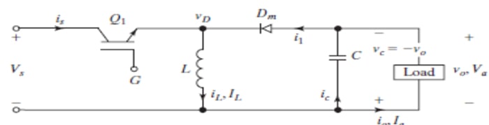
Figure 3: A Buck-Boost converter
Applications of Buck-Boost Converters
- They are suitable for extensive input voltage range and constant output voltage devices, such as regular voltage batteries, solar power generation, and power modules
- It is present in many industrial applications such as subway cars, trolleybuses, battery-powered vehicles, battery charging, etc.
- It is present In self-regulating power supplies and control applications
- It powers Active Matrix OLED displays in wearable devices
- It is present in energy harvesting systems
Advantages of Buck-Boost Converters
- It offers a higher output voltage
- It has a low operating duct cycle and low voltage on MOSFETs
- They are highly efficient and provide both buck/boost operations simultaneously
- There is an easy implementation of short circuit protection
Disadvantages of Buck-Boost Converters
- The output capacitor's continuous input current and charging current result in a larger filter size and more EMI issues
- The inverted output introduces complexity in the sensing and feedback circuit
- It suffers from poor efficiency for high gain (small or large duty cycle)
- No isolation from input to output is a critical feature in many applications
Cúk Converter
Figure 4 shows a circuit arrangement of the Cúk regulator using a power bipolar junction transistor. Like the buck-boost regulator, the Cúk regulator offers an output voltage less than or more than the input voltage. Still, the output voltage polarity is opposite to that of the input voltage. When the input voltage is on and transistor Q1 is off, diode Dm is forward biased, and capacitor C1 charges through L1, Dm, and the input supply Vs. Transistor Q1 acts as a controlled switch, and diode Dm is an uncontrolled switch. They operate as two SPST current-bidirectional switches.
Two modes run the circuit. Mode 1 begins when transistor Q1 is on at t = 0. The current through inductor L1 rises. The voltage of capacitor C1 simultaneously reverses biases diode Dm and turns it off. The energy present in capacitor C1 discharges to the circuit formed by C1, C2, the load, and L2. Mode 2 begins when transistor Q1 is off at t = t1. The capacitor C1 charges from the input supply, and then there is a transference of energy stored in the inductor L1 to the load. The diode Dm and transistor Q1 provide a synchronous switching action. The energy transfer medium from the source to the load is capacitor C1.
The output voltage is given by

Where k is the duty cycle and is given by

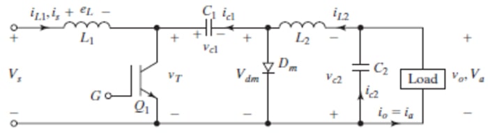
Figure 4: A Cúk Converter
Applications of Cúk Converter
- It regulates the voltage for the DC application systems
- Regulation of hybrid solar-wind energy system
- Electric vehicle (EV) technology battery management system
Advantages of Cúk Converter
- It has zero input ripple and zero output ripple features
- The output voltage can be lower or higher than the input voltage
- The inherent filtration of input and output occurs due to its topology
- The energy flow is continuous, minimizing EMI, and power flow can be bidirectional
Disadvantages of Cúk Converter
- The output voltage inverts in the non-isolated version, and the switch current stress can be high
- There is an increase in component count compared to the buck-boost topology
- The capacitor C1 is of considerable size and acts as the voltage source when the switch turns off
- The output voltage needs an inverting mechanism since the output voltage reverses compared with the input voltage
SEPIC converter
The initials SEPIC stand for “Single-Ended Primary Inductance Converter.” The Cúk converter, with its inverting buck-boost feature, exhibits non-pulsating input and output terminal currents. The single-ended primary inductance converter (SEPIC) is a noninverting Cúk converter and forms by interchanging the diode Dm and inductor L2 locations (Figure 4). Figure 5 shows the SEPIC. The Cúk and SEPIC exhibit a desirable feature: the switching MOSFET’s source terminal directly connects to the common ground. This feature simplifies gate-drive circuitry construction. The output voltage of SEPIC inverse is given by

Where k is the duty cycle and is given by


Figure 5: A SEPIC Converter
Applications of SEPIC Converter
- Battery-operated equipment and handheld devices
- NiMH chargers
- DC power supplies with a broad range of input voltages
- LED lighting applications
Advantages of SEPIC Converter
- Less space on PCB
- Less cost
- Input ripple current cancellation (results in a smaller input capacitor and an uncomplicated EMI input filter)
- Increased efficiency
Disadvantages of SEPIC Converter
- The SEPIC has a pulsating output current
- Since the SEPIC converter transfers all its energy via the series capacitor, a capacitor with high capacitance and current handling capability is required
- The fourth-order nature of the converter also makes the SEPIC converter challenging to control, making it only suitable for prolonged varying applications


